PISONICS· Xi’an Pisonics
PS7100 Series
Spectroscopic Concentration/Mass‑Density Meter
UV‑Vis‑NIR Multi‑Channel Full Spectrum + MLR Multicomponent Intelligent Modeling
Semiconductor/Wafer Wet Etching Industry Application Case
—— Simultaneous Monitoring of Multi‑Component Tank Solution Concentrations: HF + H₂SO₄ + H₃PO₄ + DI Water ——
PFA All‑Fluorine Lining · Sapphire Optical Window · Tank Solution Lifetime Management · Yield Improvement
【Key Measured Parameters: HF + H₂SO₄ + H₃PO₄ + DI Water】
Semiconductor/Wafer Wet Etching · PS7100 Multicomponent Spectral Online Analysis Solution
1. Process Background
Wet etching in the semiconductor industry is one of the critical steps in the front-end (FEOL) and back-end (BEOL) processes, primarily used for removing oxide layers from silicon wafers, patterning metal electrodes, and controlling copper interconnect sidewall etching. Typical tank solution formulations include SPM (H₂SO₄ + H₂O₂ = 4:1, photoresist removal), BHF (HF + NH₄F, buffered oxide etching), and high‑temperature phosphoric acid baths (Si₃N₄ removal), all involving precise mixing of highly corrosive chemicals such as HF, H₂SO₄, and H₃PO₄.
As wafers advance to 14 nm, 7 nm, and 5 nm process nodes, the tolerance for tank solution concentration stability has tightened from the traditional ±5% to within ±1%. Even a slight deviation in any acid’s concentration can degrade the etching rate and pattern accuracy, thereby reducing device yield (in the FAB industry, each percentage point drop in yield typically translates to a 0.5%–1% loss in revenue). Moreover, during operation, tank solutions continuously drift due to water evaporation, dissolution of silicon or metals, and byproduct formation, necessitating accurate determination of the “effective lifespan” of the bath—changing it too early wastes expensive chemicals, while delaying replacement harms yield.
2. Pain Points of Traditional Analysis Methods
• In semiconductor wet processes, 3–4 components such as HF, H₂SO₄, H₃PO₄, and DI water often need to be monitored simultaneously; conventional offline analysis requires four sampling events plus four sets of laboratory equipment, with each analysis taking several hours;
• HF readily corrodes common materials like glass, quartz, and stainless steel—traditional contact instruments have extremely short probe and membrane lifetimes, and failure can contaminate wafer batches (each FAB batch is worth hundreds of thousands of yuan);
• Manual sampling carries risks of HF‑related burns and H₂SO₄‑induced scalds; given the strict access controls in semiconductor FABs, frequent sampling is unacceptable;
• Estimating tank solution life relies on empirical judgment—changing the bath too early wastes high‑purity chemicals (electronic‑grade HF costs about 80,000 yuan per ton), while delaying replacement hurts product yield, leaving FAB managers in a long‑standing dilemma.
3. PS7100 Solution
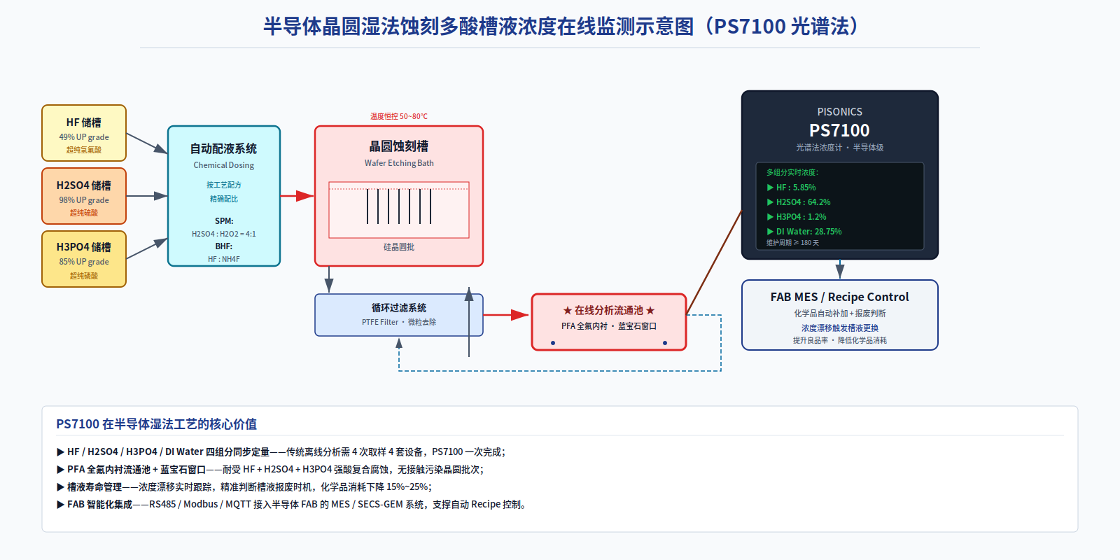
The PS7100 is installed on a bypass flow cell in the circulating filtration system of the wafer etching tanks, featuring a composite structure with PFA all‑fluorine lining and sapphire optical windows, capable of withstanding the combined corrosive effects of HF, H₂SO₄, H₃PO₄, and other acids. By acquiring full UV‑Vis‑NIR spectra and employing MLR intelligent modeling, a single measurement simultaneously outputs the real‑time concentrations of HF, H₂SO₄, H₃PO₄, and DI water, providing second‑level feedback to the FAB’s MES and recipe control systems.
Figure 1: Online Concentration Monitoring Scheme for Multi‑Acid Tank Solutions in Semiconductor Wafer Wet Etching
Core Technical Value of the PS7100 in Semiconductor/Wafer Wet Etching ▶ Simultaneous quantitative measurement of four components—HF, H₂SO₄, H₃PO₄, and DI water—on a single instrument; traditional offline analysis requiring four separate tests is replaced by a single run with the PS7100. ▶ PFA fully fluorinated-lined flow cell with sapphire optical windows—resistant to HF and multi-acid corrosive mixtures, ensuring no contact contamination of wafer batches. ▶ Precise management of bath life—real-time monitoring of concentration drift enables accurate determination of the optimal time for fluid replacement, reducing chemical consumption by 15%–25%. ▶ FAB intelligent integration—RS485/Modbus/MQTT connectivity to the FAB’s MES/SECS‑GEM systems, supporting automated recipe control. ▶ Maintenance interval ≥ 180 days—long-life OLED light source combined with a purely optical design, resulting in extremely low failure rates and meeting FAB high-availability requirements. ▶ Optional Ex db ib IIC T6 Gb explosion-proof version—suitable for hazardous-area operations in gas storage and solution preparation stations around semiconductor FABs. |
4. Customer Value
Comparison Dimensions | Original offline/contact-based solution | PS7100 Spectroscopic Solution |
Multicomponent Capability | 4 samples + 4 sets of equipment | Single measurement of four components |
HF-resistant | Conventional instruments have a short service life | PFA + sapphire ≥ 180 days |
Batch Contamination Risk | Contact-type devices pose a leakage risk | Optical non-contact · Zero contamination |
Timing for Liquid Exchange | Empirical estimation · High wastage | Accurate determination of concentration drift |
Chemical Consumption | Baseline 100% | Reduce by 15%–25% |
FAB Integration | Local instruments · Difficult to automate | Direct integration with MES/SECS-GEM |
Yield Impact | Tank-liquid fluctuations → Yield fluctuations | Electroplating bath stability → Yield improvement |
At a leading domestic 12‑inch wafer foundry, the PS7100 was deployed in the circulation loops of the BHF buffered etching tank and the SPM resist‑removal tank, enabling simultaneous real‑time monitoring of HF, H₂SO₄, H₃PO₄, and DI water. After 12 months of operation, feedback indicates that high‑purity chemical consumption decreased by approximately 18% (saving about 6 million yuan annually), the effective service life of the tank solution extended by 22%, and etching rate fluctuations narrowed from ±4% to within ±1.2%, resulting in an approximate 0.8 percentage point increase in process‑stage product yield. This solution has since been adopted in various niche applications, including LED sapphire substrate etching, PCB plating bath formulation, and texturing of silicon wafers for solar cells.
Conclusion
Based on the four ultrasonic and optical measurement principles of the PS70 series—acoustic impedance, acoustic attenuation, sound velocity, and spectroscopy—Xi’an Pisonics (PISONICS) has developed a comprehensive portfolio of process analytical instruments covering all operating conditions and precision levels, ranging from solid‑liquid two‑phase slurries (PS7000) and clean homogeneous liquids (PS7020) to multicomponent complex media (PS7100). Among these, the PS7100 spectroscopic concentration/mass‑density meter, equipped with a full‑band UV‑Vis‑NIR LED array, multi‑channel detectors, and an MLR intelligent modeling algorithm, uniquely offers the capability to quantitatively determine the concentrations of multiple chemical components in a single instrument—something neither acoustic impedance nor sound velocity methods can achieve.
Tailored to the process characteristics of the semiconductor and wafer wet etching industries, the PS7100 spectroscopic concentration/mass‑density meter provides end‑to‑end technical support, from selecting the optical probe (contact material, light path length, explosion‑proof rating), designing the flow cell (with clamps, flanges, or PFA lining), calibrating the MLR model, to integrating with DCS, MES, and LIMS systems. For in‑depth discussions on your specific project conditions, customized MLR calibration, or on‑site commissioning services, please feel free to contact the Xi’an Pisonics technical team at any time.